1997 Mar 03 3
Philips Semiconductors Product specification
Video output amplifier TDA6106Q
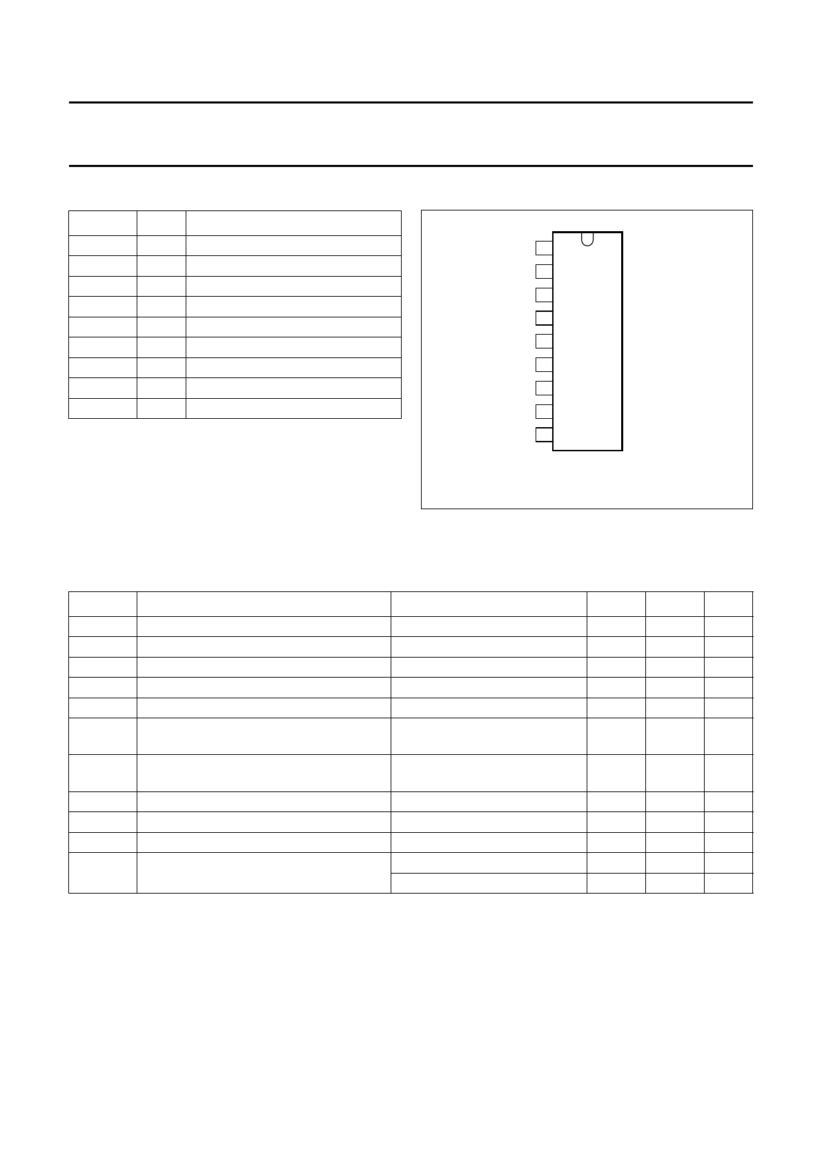
PINNING
SYMBOL PIN DESCRIPTION
n.c. 1 not connected
n.c. 2 not connected
V
in
3 inverting input voltage
GND 4 ground, substrate
I
om
5 black current measurement output
V
DD
6 supply voltage
n.c. 7 not connected
V
oc
8 cathode output voltage
V
of
9 feedback output voltage
Fig.2 Pin configuration.
handbook, halfpage
TDA6106Q
MBG342
1
2
3
4
5
6
7
8
9
n.c.
n.c.
V
in
GND
I
om
V
DD
n.c.
V
oc
V
of
LIMITING VALUES
In accordance with the Absolute Maximum Rating System (IEC 134); voltages with respect to pin 4 (ground) unless
otherwise specified; currents specified as in Fig.1.
Notes
1. The cathode output is protected against peak currents (caused by positive voltage peaks during high-resistance
flash) of 5 A maximum with a charge content of 100 µC.
2. The cathode output is also protected against peak currents (caused by positive voltage peaks during low-resistance
flash) of 10 A maximum with a charge content of 100 nC.
3. Human body model: equivalent to discharging a 100 pF capacitor through a 1.5 kΩ resistor.
4. Machine model: equivalent to discharging a 200 pF capacitor through a 0 Ω resistor.
SYMBOL PARAMETER CONDITIONS MIN. MAX. UNIT
V
DD
supply voltage 0 250 V
V
in
inverting input voltage 0 8 V
V
om
black current measurement output voltage 0 6 V
V
oc
cathode DC output voltage 0 V
DD
V
V
of
feedback output voltage 0 V
DD
V
I
oc(l)
low non-repetitive peak cathode output
current
flashover discharge = 100 µC;
note 1
05A
I
oc(h)
high non-repetitive peak cathode output
current
flashover discharge = 100 nC;
note 2
010A
P
max
maximum power dissipation 0 tbf W
T
stg
storage temperature −55 +150 °C
T
j
junction temperature −20 +150 °C
V
esd
electrostatic discharge note 3 −2000 +2000 V
note 4 −300 +300 V


