I/O Ports
15-28
15.6.3 Pin Configurations
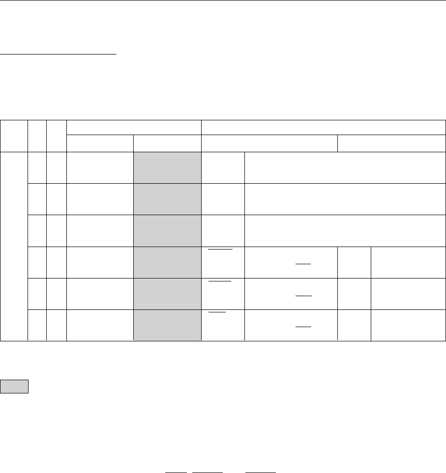
Table 15-6-1 shows the pin configurations for port 4.
Table 15-6-1 Port 4 Configuration
Port Pin P4n P4nM = "1" P4nM = "0"
No. P4nD = "1" P4nD = "0" P4nS = "1" P4nS = "0"
Port 4 75 P40 General-purpose General-purpose SBT0
*1
Serial 0 transfer clock input/output
output port input port
74 P41 General-purpose General-purpose SBI0 Serial 0 data input
output port input port
73 P42 General-purpose General-purpose SBO0
*1
Serial 0 data input/output
output port input port
71 P43 General-purpose General-purpose DCAS0 DRAM CAS signal 0 SBT1
*2
Serial 1 transfer
output port input port output (for 2CAS) clock input/output
70 P44 General-purpose General-purpose DCAS1 DRAM CAS signal 1 SBI1 Serial 1
output port input port output (for 2CAS) data input
68 P45 General-purpose General-purpose DWE DRAM write signal SBO1
*2
Serial 1
output port input port output (for 2CAS) data input/output
[Note 1]
: When reset (whether in address/data separate mode or address/data multiplex mode)
*1 : The input/output setting is made through the serial interface 0 settings.
*2 : The input/output setting is made through the serial interface 1 settings.
Note: For details on the serial interface settings, refer to chapter 13, "Serial Interface."
[Note 2]
When the bus authority is granted, DWE, DCAS1, and DCAS0 go to high impedance.


