KP915GV Product Manual
25
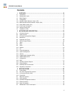
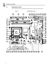
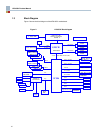
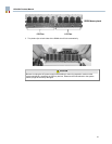
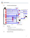
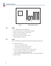
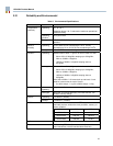
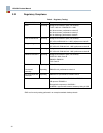
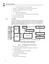
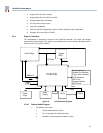
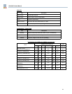
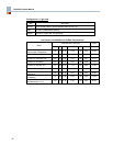
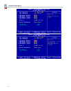
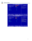
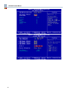
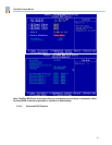
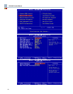
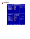
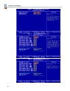
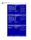
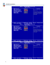
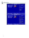
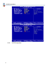
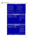
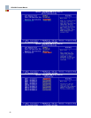
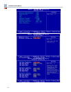
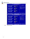
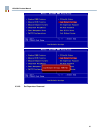
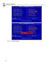
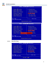
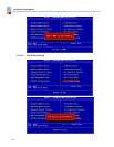
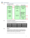
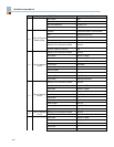
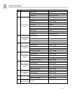
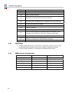
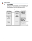
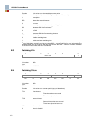
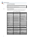
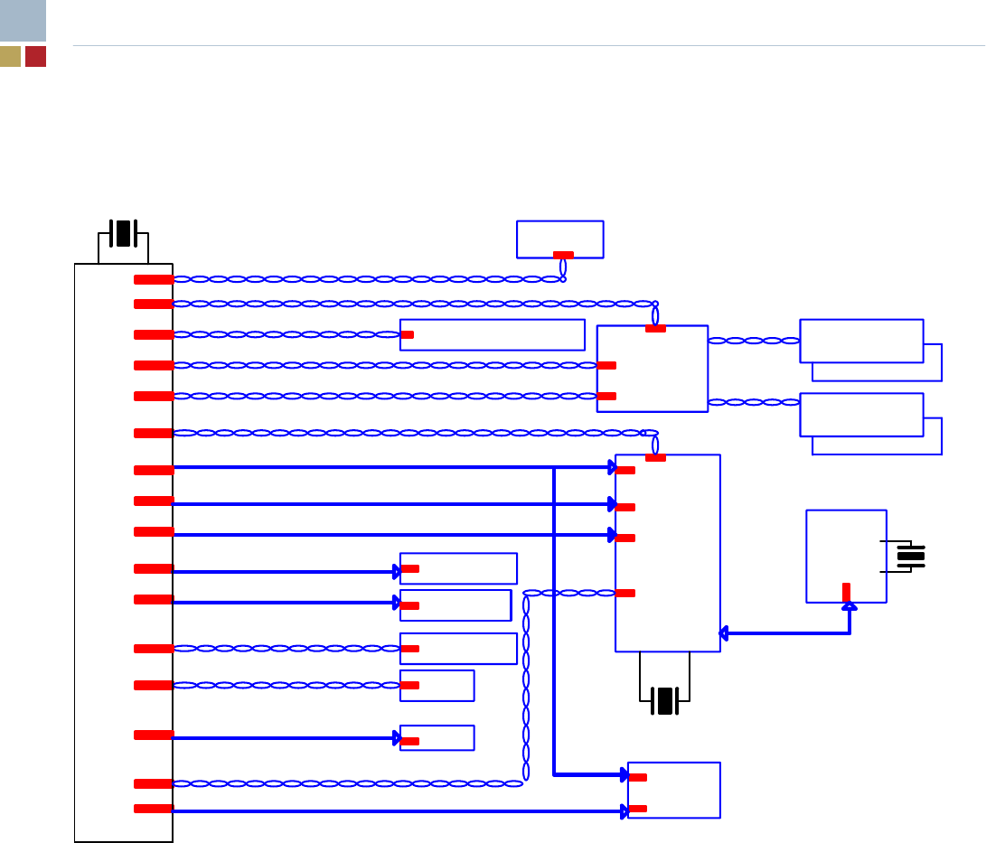
2.3 On board Clocking Block Diagram
PCI Express x16 SDVO
PCI Express/DMI 100 MHz Diff Pair
USB/SIO 48 MHz
PCI Express 100 MHz Diff Pair
ICH 33 MHz
MCH 133/200 MHz Diff Pair
REF 14 MHz
SATA 100 MHz Diff Pair
PCI-E SLOT
1,2
PCI Express 100 MHz Diff Pair
PCI 33 MHz
LAN
CPU 133/200 MHz Diff Pair
PCI Express 100 MHz Diff Pair
Super I/O
Azalia Bit Clock
FWH
CPU
DDR 4 Slots 12 Diff Pair CLKs
CK-410
Channel B DDR2
ICH6
Channel A DDR2
GMCH
Grantsdale
SIO 33 MHz
32.768KHz
DIMM2
1394 33 MHz
1394
14.318MHz
DIMM1
Azalia
24.576MHz
DIMM2
FWH 33 MHz
PCI Slot
1,2&3
DIMM1
PCI Express/DMI 100 MHz Diff Pair
DOT 96 MHz Diff Pair
Figure 4. Clocking Block Diagram
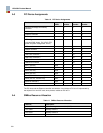
2.4 Mechanical
• Compliant with the ATX 2.03 specification
• Lead-free design
• 4-layer PCB, components top side only, immersion silver surface finish
• Screen printing includes RadiSys product code, RadiSys part number, RadiSys branding,
selected component reference designators, and UL and WEEE directive logos.
2.5 Expansion Slot Types