KP915GV Product Manual
38
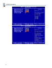
• 5V tolerant buffers on IDE, PCI, and Legacy signals
• Integrated 1.5V Voltage Regulator (INTVR) for the Suspend and LAN wells
• Firmware Hub I/F supports BIOS Memory size up to 8 MBytes
• Low Pin Count (LPC) I/F
• Supports two Master/DMA devices
• Support for Security Device (Trusted Platform Module) connected to LPC
• GPIO, TTL, Open-Drain, Inversion
• Package 31x31 mm 609 pin mBGA
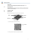
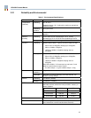
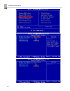
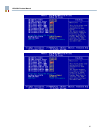
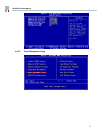
3.2.2 Flash BIOS
The SST 49LF004B (512K x 8) 4Mb Flash EEPROM, This flash memory device is designed to
interface with host controllers (chipsets) that support a Low Pin Count (LPC) interface for BIOS
applications. The SST49LF004B devices comply with Intel’s LPC Interface Specification 1.1,
supporting single-byte Firmware Memory and LPC Memory cycle types. It as a flash BIOS and it
will be implemented via the NS PC8374K Super I/O.
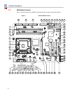
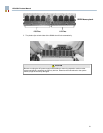
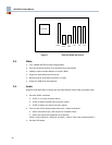
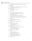
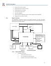
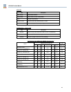
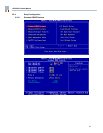
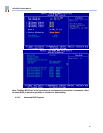
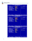
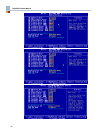
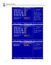
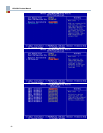
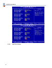
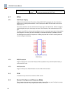
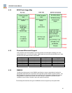
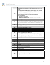
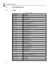
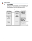
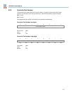
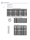
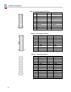
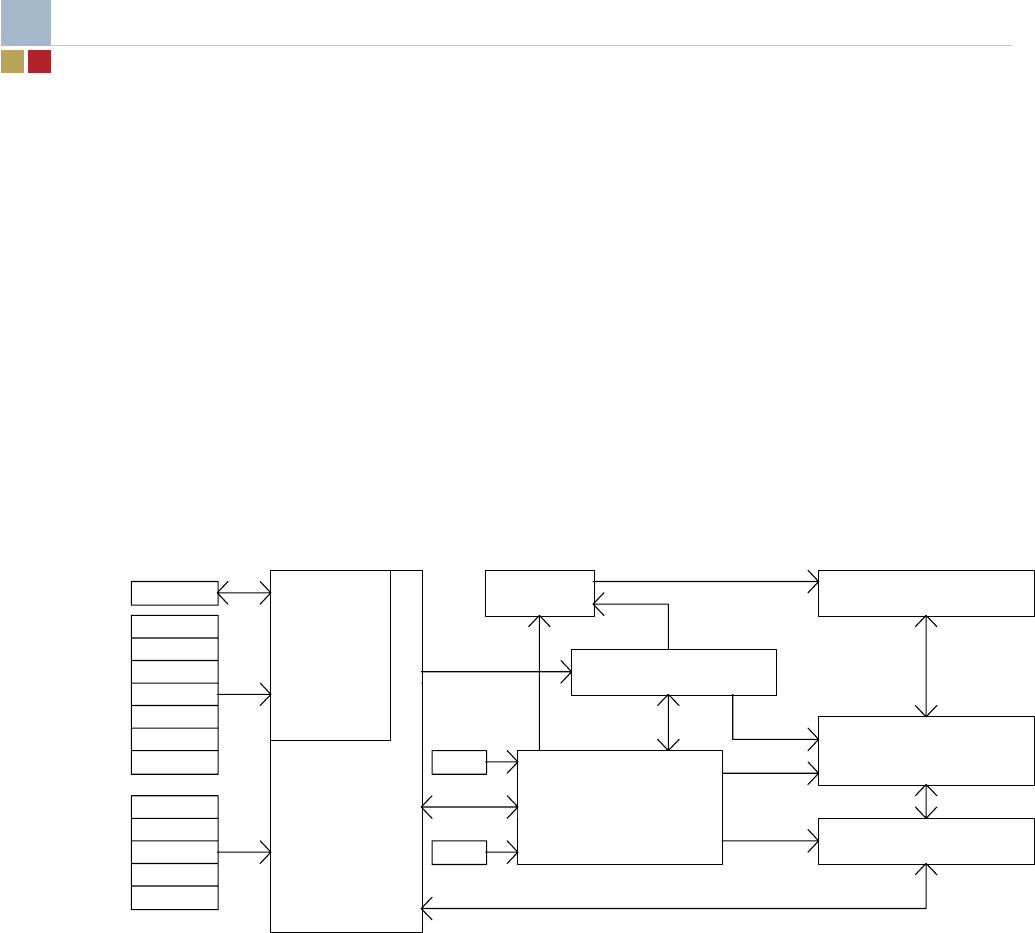
Memory
Superflash
X-Decoder
Address Buffers & Latches
Interface
FWH/LPC
GPI[4:0]
ID[3:0]
LFRAME#
LCLK
LAD[3:0]
Control Logic
I/O Buffers and Data Latch
Y-Decoder
TBL#
Programmer
WE#
QE#
DQ[7:0]
A[10:0]
R/C#
Interface
INIT#
WP#
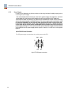
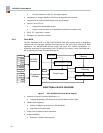
FUNCTIONAL BLOCK DIAGRAM
RST#
MODE
Figure 7. SST 49LF004B Functional Block Diagram
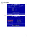
• Conforms to Intel LPC Interface Specification 1.1
• Supports Single-Byte LPC Memory and Firmware Memory Cycle Types
• Flexible Erase Capability
• Uniform 64 KByte overlay blocks for SST49LF004B
• Chip-Erase for PP Mode Only
• Single 3.0-3.6V Read and Write Operations
• Superior Reliability
• Endurance: 100,000 Cycles (typical)