KP915GV Product Manual
44
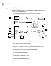
• Heceta6-compatible register set accessible via the LPC interface and SMBus
• Supports the following combinations of LMxx devices:
• LM41 and optional LM30
• LM32
• LM40
• Simultaneous read support via LPC interface and SMBus
• Generates SMI on critical temperature event
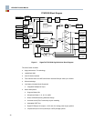
3.3.4.2 Glue Functions
•
Flash Write Protect control (using GPIO) with optional SMI generation when
cleared
• Floppy Disk Drive Write Protect (WGATE) lockable control (cleared only by
hardware reset)
• Generates the power-related signals:
• Main Power good
• Power distribution control (for switching between Main and Standby
regulators)
• Resume reset (Master Reset) according to the 5V standby supply status
• Main power supply turn on (PS_ON)
• Voltage translation between 2.5V or 3.3V levels (DDC) and 5V levels (VGA) for
the SMBus serial clock and data signals
• Isolation circuitry for the SMBus serial clock and data signals
• Buffers PCI_RESET to generate three reset output signals
• Buffers PWRGD_PS to generate IDE reset output.
• Generates “highest active supply” reference voltage
• Based on 3.3V and 5V Main supplies
• Based on 3.3V and 5V Standby supplies
• High-current LED driver control for Hard Disk Drive activity indication
• Software selectable alternative functionality, through pin multiplexing
3.3.4.3 General-Purpose I/O (GPIO) Ports
•
All 16 GPIO ports powered by Voltage Standby 3V (VSB3)
• Each pin individually configured as input or output
• Programmable features for each output pin:
• Drive type (open-drain, push-pull or TRI-STATE)
• TRI-STATE on detection of falling VDD3 for VSB3-powered pins driving
VDD-supplied devices
• Programmable option for internal pull-up resistor on each input pin (some with
internal pull-down resistor option)